|
How Do I Configure the A7’s SDRAM Interface in FastChip?
Configuring the A7’s SDRAM interface in FastChip proves to
be a bit confusing to most FastChip users.
There are two places during the FastChip development flow
where you need to make choices about your SDRAM subsystem architecture.
The first selection occurs within FastChip. For example,
let’s assume that your design requires an 8Mx32 SDRAM subsystem, using a
single SDRAM bank.
 Select Constraints à
I/O Editor from the FastChip menu bar or click the I/O Editor button. Select Constraints à
I/O Editor from the FastChip menu bar or click the I/O Editor button.
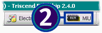
 From the I/O Editor toolbar, click MIU. From the I/O Editor toolbar, click MIU.
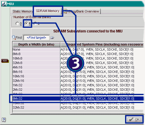
 Under the MIU settings, click the SDRAM Memory tab.
Select 1 external memory bank and set the memory depth and width to 8Mx32.
Click OK when finished. Under the MIU settings, click the SDRAM Memory tab.
Select 1 external memory bank and set the memory depth and width to 8Mx32.
Click OK when finished.
 Depending on your previous design, you may need to re-Bind your
project. When you change the MIU settings, FastChip may reserve some PIO
pins so that they can connect to your SDRAM subsystem. Depending on your previous design, you may need to re-Bind your
project. When you change the MIU settings, FastChip may reserve some PIO
pins so that they can connect to your SDRAM subsystem.
The second selection occurs in FastChip Device Link (FDL).
 Invoke FastChip Device Link (FDL), if not already open. Invoke FastChip Device Link (FDL), if not already open.
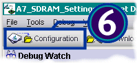
 Click Configuration in FDL’s toolbar to create a configuration
image..\ Click Configuration in FDL’s toolbar to create a configuration
image..\
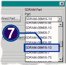
 Under SDRAM Part, select the appropriate SDRAM device for your
application. For example, the SDRAM memory subsystem was already defined to be 8Mx32 from within FastChip.
Assume that this 8Mx32 subsystem is built from 10 ns, 128Mbit SDRAMs with a
x16 interface. This means that each device is organized as 8Mx16. The part
in the droplist matching these specifications is SDRAM-08M16-10. Under SDRAM Part, select the appropriate SDRAM device for your
application. For example, the SDRAM memory subsystem was already defined to be 8Mx32 from within FastChip.
Assume that this 8Mx32 subsystem is built from 10 ns, 128Mbit SDRAMs with a
x16 interface. This means that each device is organized as 8Mx16. The part
in the droplist matching these specifications is SDRAM-08M16-10.
 Click OK to save these configuration settings and to create a
configuration image ready for download. Click OK to save these configuration settings and to create a
configuration image ready for download.
So why is it a two-step process?
FastChip is intended to capture the general configuration
of the design—i.e., the SDRAM interface is a single 8Mx32 bank of SDRAM.
FastChip Device Link (FDL) is where you choose the
specific devices that make up the memory subsystem. In this example, we
chose 10 ns, 128Mbit SDRAMs organized as 8Mx16. However, you might only have
7.5 ns devices in inventory. With a simple change in FDL, we can create a
new configuration file, optimized for the faster speed grade without
affecting the remainder of the design.
|
FastChip Version: 2.4.0
This solution may or may not apply to other versions
of the FastChip development system.
|
 ® ®
©
2002 by Triscend Corporation. All
rights reserved.
|